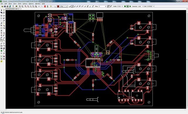
PCB Trace Routing is very similar to road planning. You have a board which connects many electrical components into one whole. What links these elements are traces that function very similarly like a road.
They lead electricity throughout the electrical components, which in turn makes them function. It is very similar to the traffic in the city. Much like how the overload of traffic; traffic jams, affect the city, the same happens on PCBs.
That’s why it’s vital to know how the PCBs function, and how to optimize the PCB trace routing to perfection. Okay, you cannot go perfect, but you can come pretty close to it for sure!
Much how road designers analyze the traffic potential in the city, it is the same with PCB designers. You have to know where you want the traffic to go, to avoid unnecessary errors or “traffic jams”.
Careful planning can minimize these errors, much like how it has helped in city traffic greatly. Now that you see how PCB trace routing is essential for electric devices to function correctly, let’s talk a bit about how to make it better.
Main Attributes to Keep Note Of
As the PCB traces are much similar to the city traffic, you must know something about the essential attributes if you want them to function properly. So, the first step in efficient PCB trace routing is to analyze these essential attributes and know how to utilize them properly. You want to avoid as many traffic jams as you can, don’t you?
Pad Size
This is your workspace when you’re looking for a printed circuit board. The thing you have to know about this is that the larger pads naturally give you more workspace, but you have to keep note of the pad distance too. Larger gaps between pads open up more possibilities for solder bridge shorts, and you want to prevent that from happening.
Trace Width
It is almost the same as the road width. You have to plan how much traffic can the road carry and adjust the road width accordingly. The same is with the electrical currents that flow through PCB traces. You have to watch out that you don’t overload the traces, as that will cause a sort of traffic jam on the PCB. The best idea is to strike a perfect balance to keep the electricity flowing at a reasonable speed while decreasing circuit shorts.
Connections
The risk of circuit shorts increases proportionally with the number of connections that go to a pad or a node on the PCB. When trace paths branch, they are closer to each other and accumulate a stronger electrical charge. The most common way to connect the components on the pad is the uneven solder paste. That, in turn, produces solder bridges that connect different pads. You should also give extra caution to outputs if you want to reduce the number of circuit shorts and improve the functionality of the PCB.
Consistent Trace and Pad Size
Use different types of traces and pads, and you’ll experience more functionality errors. If you want to control the number of these errors, then you should definitely implement consistent size to these components. This notion comes pronounced when using multi-layer boards, as they are more complex, and that also means that finding errors is also much more complicated.
Corners
Sharp corners can cause lots of disturbances in the city traffic, and it’s the same with the printed circuit boards. In road design, round corners are implemented to decrease these disturbances drastically. With sharp corners, the risk of circuit shorts on the PCB are much higher, and applying the same design choice we mentioned is the key to improve its functionality.

Ways to Improve PCB Trace Routing
The people who cause traffic disturbances are often those that haven’t familiarized themselves with the basic principles of car traffic. You can say that the same things happen to printed circuit board designers – the lack of knowledge and experience.
When you know what actually affects the trace routing, then you can implement better design choices that will enhance the functionality of your PCB.
The most important part, before you start with trace routing, is to verify the limits for trace width and pad spacing of the desired manufacturer. You don’t want to be doomed from the beginning, don’t you?
To avoid the unnecessary short circuits, you have to analyze the load that the traces will come into, and adjust the trace width accordingly.
When you don’t need narrow trace routes and spaces, don’t hesitate to implement their broader counterparts. It saves a lot of time for you and decreases the costs significantly.
The most natural thing is to keep trace routes short and direct so that you can control them with less effort. To do that, you need to group electric components that are related, so that you can determine the source of functionality error easier. You should also avoid sharp corners to decrease the amount of circuit shorts on the board.
These design choices will significantly affect the PCB trace routing, for the better. With this information in your mind, you can now design PCBs that are more functional than ever!

